Overview
One of the key features that differentiates the Intel SoC platforms from similar SBCs (Single Board Computers) like the Raspberry Pie is that the Intel SoC has a built in FPGA. This unique feature allows developers to design custom peripheral devices or hardware accelerators. The ability to define custom peripherals in “hardware” lessens the computational load in software and provides stricter control in situations where exact timing is critical. The peripheral devices are designed in Verilorg (or VHDL) and can be accessed from the ARM Cortex-A9 core.
Accessing Peripheral Devices in the FPGA
When Linux (running on the A9 ARM cores) needs to access the FPGA, it does so by reading/writing to s specific memory location. This memory location is mapped to a special data bus called the Avalon interface. This is a custom Intel(Altera) interface that takes care of all of the messy details of synchronizing data across two clocking domains (ARM Core and FPGA). The Avalon Interface consists of the following signals:
| Signal | Description |
| address[4:0] | A subset of the FPGA’s location in the A9’s memory map. In our case, this is the lower 5 bits of the address. |
| read | When equal to 1, the operation is a read operation. |
| write | When equal to 1, the operation is a write operation. |
| readdata[31:0] | When the read signal is a 1, the peripheral will drive data on this bus that is determined by the address bus. When the read signal is a 0, the peripheral tri-state the bus. |
| writedata[31:0] | When the write signal is a 1, the peripheral will take the data found on the writedata bus and save it into the register indicated by the address bus. |
| byteenable[3:0] | Used to indicate if the operation is a byte (8-bits) , half word(16-bits), or word (32-bit) data transaction. |
When software writes to a location in the FPGA, the write signal will be asserted to a 1. At this point, it’s up to the peripheral to decide what is done with the data placed on the writedata bus. In most situations, the data will be written to a register that is defined within the peripheral. The same is true when a read of the FPGA peripheral is made. The read signal is asserted to a 1 and the peripheral will drive data onto the readdata bus so that the ARM core can access the data in the peripheral devices register set.
Implementing an Avalon Peripheral in Verilog
1. Using the information about the Avalon interface, we can create a custom peripheral device that can be added to the programmable logic of the SoC. You will first need to download the the ECE453 base project. Extract the project into a folder. We will use C:Usersece453Documentsexample_project
The ECE453 base project has a few modification to the DE1-SoC project that ships with the DE1.
- This project has the required VGA frame buffer logic added to support video on Linux
- There are I2C/SPI/UART peripherals that are part of the HPS (ARM A9 CPU) that have been routed through the FPGA to the GPIO headers found on the DE1.
3. In a text editor, open C:Usersece453Documentsexample_projectipexample_peripheralexample_peripheral.v
/*

  Author:  Your Name
  Date:  mm/dd/yyyy

*/

module example_peripheral(
  // signals to connect to an Avalon clock source interface
  clk,
  reset,
  // signals to connect to an Avalon-MM slave interface
  address,
  read,
  write,
  readdata,
  writedata,
  byteenable,
  // Non-Avalon Interface IO
  gpio_inputs,
  gpio_outputs,
  irq_out
);
The code above is the interface for our peripheral device. Like any synchronous circuit, we need a clock and areset . The next six signals define the rest of the Avalon interface described above. gpio_inputs ,gpio_outputs , and irq_out are non-Avalon related signals that we can use to interface with other modules or devices connected to the GPIO pins of the SoC. For the purposes this peripheral module, what is connected to these inputs/outputs is somewhat irrelevant. Later we will connect gpio_inputs to some push buttons and also connect gpio_outputs to some LEDs on the DE1-SoC. These connections will be made at a higher level of HDL. irq_out will not be used in this example.
4. Now lets examine some required statements in our Verilog module.
  //*******************************************************************
  // Module Interface
  //*******************************************************************
  input clk;
  input reset;

  // slave interface
  input [4:0] address;
  input read;
  input write;
  output wire [31:0] readdata;
  input [31:0] writedata;
  input [3:0] byteenable;

  input [31:0] gpio_inputs;
  output [31:0] gpio_outputs;
  output wire irq_out;

  //*******************************************************************
  // Register Addresses
  //*******************************************************************
  localparam	DEV_ID_ADDR	    = 5'b0000;
  localparam	GPIO_IN_ADDR	= 5'b0001;
  localparam	GPIO_OUT_ADDR	= 5'b0010;

  //*******************************************************************
  // Register Set
  //*******************************************************************
  reg  [31:0] dev_id_r;
  reg  [31:0] gpio_in_r;
  reg  [31:0] gpio_out_r;

   //*******************************************************************
  // Wires/Reg
  //*******************************************************************
  wire  [31:0] gpio_in;
  wire  [31:0] gpio_out;
Most of these statements are required to define if a signal is an input or an output signal. The code that is of interest is near the bottom of this section. You will see that three registers have been defined in our peripheral (all end in an _r ). In order to do that, we will define unique addresses for each register as a localparam . We also define a three reg instances to instantiate the registers themselves.
5. Next, we will allow 1 of our 3 registers to drive data on the readdata bus of the Avalon interface. The code below implements an address decoder for our 3 registers. The address signal acts as the input to the address decoder. When the readdata signal is active, the decoder will select which register places data on the Avalon readdata bus.
  //*******************************************************************
  // Register Read Assignments
  //*******************************************************************
  assign readdata =
        ( (address == DEV_ID_ADDR )    && read )  ? dev_id_r :
        ( (address == GPIO_IN_ADDR )   && read )  ? gpio_in_r :
        ( (address == GPIO_OUT_ADDR )  && read )  ? gpio_out_r : 32'h00000000 ;R )  && slave_read )  ? gpio_out_r : 32'h00000000 ;
6. The next section of HDL that we will add generates the input logic for the registers.
  // Input signals for registers
  assign gpio_in        = gpio_inputs;
  assign gpio_out       = ( (address == GPIO_OUT_ADDR )   && write ) ? writedata : gpio_out_r;
These statements determine what the next state of each register will be. gpio_inputs provides the next value of the gpio_in_r register, so on every clock cycle, the register’s value is updated with whatever values is supplied on gpio_inputs. We will see later, gpio_inputs can be connected to the slide switches on the DE1-SoC. When software wants to determine the value of the switches, it can simply read the value of the gpio_in_r register.
For gpio_out_r , the register will take on a new value when the slave_address is equal to GPIO_OUT_ADDR AND there is a write operation currently active. This situation occurs when software writes a new value to the register. If software is not currently trying to change the value being driven, the register keeps is current value.
7. Now we will add the HDL that will determine the non-Avalon output signals.
  // Output signals to external devices.
  assign gpio_outputs = {gpio_out_r[31:0]};
  assign irq_out = 1'b0;
We are not presently using the interrupt, so we force its value to a 0. The value on gpio_outputs is simply the value held in the registergpio_out_r .
8. Our final segment of code implements the synchronous block of logic required to properly synthesize a register set. It should be noted that this example employs a coding style that separates the combinational logic used to determine the next state from the always block used to implement the flip flops for the register. While it might seem less convenient, it is a best practice that results in HDL that not only simulates correctly, but also is synthesizes correctly.
  //*******************************************************************
  // Registers
  //*******************************************************************
  always @ (posedge clk or posedge reset)
  begin
    if (reset == 1)
    begin
      dev_id_r    <= 32'hECE45318;
      gpio_in_r   <= 32'h00000000;
      gpio_out_r  <= 32'h00000000;
    end

    else
    begin
      dev_id_r    <= 32'hECE45318;
      gpio_in_r   <= gpio_in;
      gpio_out_r  <= gpio_out;
    end
  end

endmodule
You can download a completed copy of this file here. If you are writing your own HDL, I would strongly suggest simulating your peripheral before moving on. The Quartus build process can take anywhere from 5-15 minutes to complete, so you will want to simulate first and fix any logic errors before you attempt to build the programming file.
Adding a Peripheral To Content Library
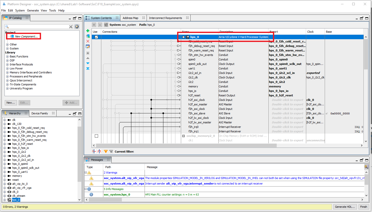
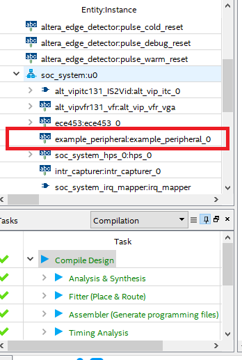
1. In order to add a custom peripheral device to our design, we will need to use the Platform Designer tool. You can find Platform Designer under “Tools” on the top menu in Quartus. When Platform Designer opens, select soc_system.qsys from the Open dialog. You should see the following representation of the base Altera SoC system. The ARM-A9 processor is (called hps_0) in the structure below.
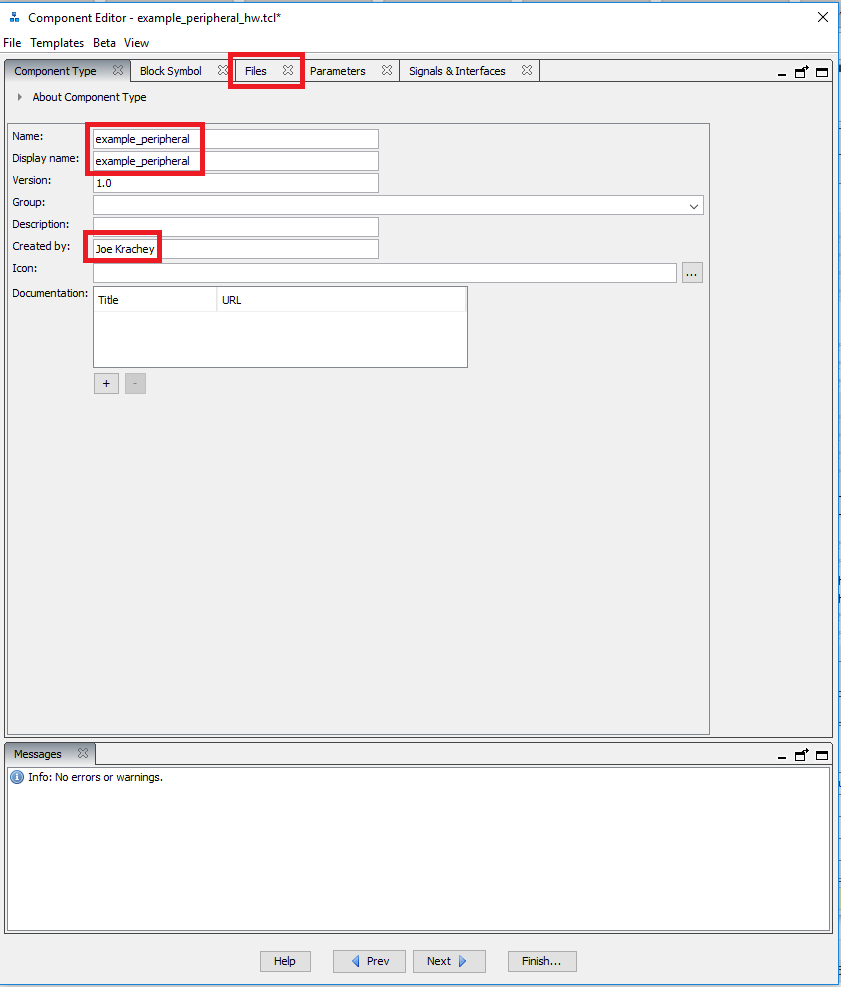
2. We will add a new peripheral by double clicking on “New Component“. From the Component Editor window, fill in the name of the component and the display name. When you are done, click on the files tab.
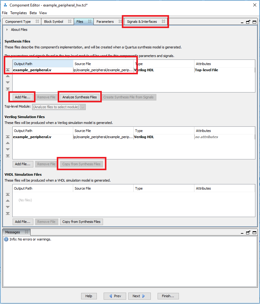
3. Click on the Add File… button near the Synthesis Files area and navigate to the example_peripheral.v file you created above.
4. After you have selected this file, click the Analyze Synthesis Files.
5. Click on the Copy from Synthesis Files Button under Verilog Simulation Files.
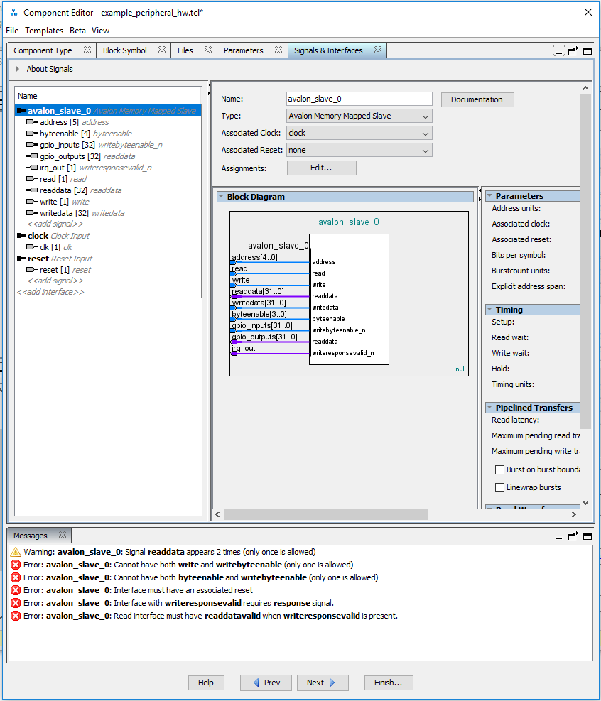
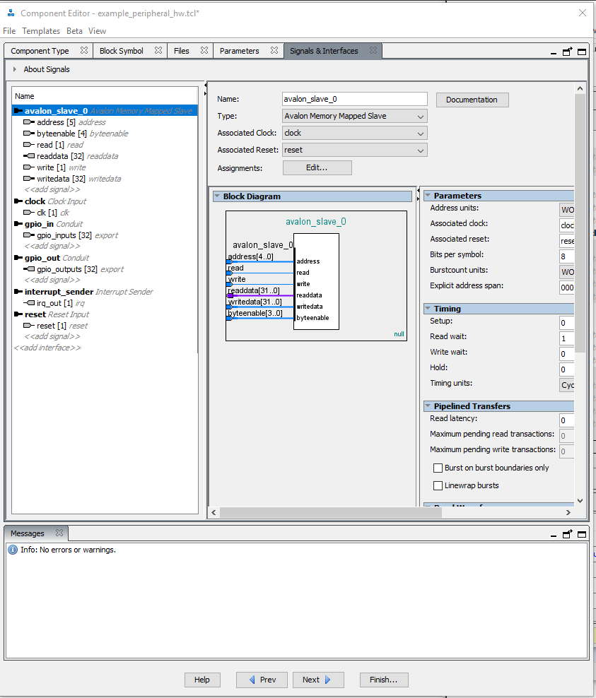
6. Now click on the Signals & Interfaces tab.
7. You will now have to identify the purpose of all the input and output signals of the peripheral. As you can see, Platform Designer figures out most of the connections, but there are a few changes that will need to be made. Platform Designer didn’t know what to do with gpio_inputs ,gpio_outputs , and irq_out because they are not part of the standard Avalon interface. There is also an error about the Avalon interface needing an Associated Reset. Currently, it is listed as none.
8. Let’s start by selecting the Associated Reset and changing it from none to reset.
9. Create a Conduit interface for both the gpio_inputs and gpio_outputs buses. We can do this by double clicking on the <<add interface>> found after all the signals. You should select an interface type as Conduit.
10. After you have created the new Conduit, double click on the interface named conduit_end and change the name to be gpio_out.
11. After you have changed the name, select the gpio_outputs[32] signal listed under the avalon_slave_0 interface and drag it so that it is listed as part of the gpio_out conduit.
12. When you have selected the gpio_outputs[32] signal, change the Signal Type to be “export“. You can type export into the dialog box for Signal Type.
13. Create a new Conduit. Double click on the interface named conduit_end and change the name to be gpio_in.
14. After you have changed the name, select the gpio_inputs signal listed under the avalon_slave_0 interface and drag it so that it is listed as part of the gpio_in conduit.
15. When you have selected the gpio_inputs[32] signal, change the Signal Type to be “export“. You can type export into the dialog box for Signal Type.
16. Double clicking on the <<add interface>> found after all the signals. This time, select Interrupt Sender as the interface type.
17. Select the irq_out signal listed under the avalon_slave_0 interface and drag it so that it is listed as part of the interrupt_sender.
18. With irq_out[1] selected, change the Signal Type to be irq.
At this point, your Component Editor Window should look like this:
19. Click the Finish button.
20. Select Yes to save the component.
Adding A Custom Component to the SoC
1.Under the Project Tab, you should see a new component type called example_peripheral. Double click this to add a new instance of example_peripheral to the SoC.
2. From the dialog that pops up, select Finish.
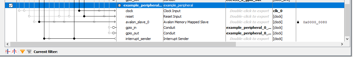
3. Scroll down to the bottom of the System window.
4. We now need to connect the inputs/outputs of the example_peripheral to the other resources in the SoC. Let’s start by connecting the clock input to the clk_0.clk signal. You can do this by clicking on the second bubble to the left of the clock.
5. Connect the reset signal up to the clk_0.clk_reset signal (2nd Bubble from the left).
6. Connect the avalon_slave_0 interface to the soc_system.hps_0.h2f_lw_axi_master bus. (4th Bubble from the left).
7. In the ECE453 base project, we already have another custom peripheral defined at offsett 0x0000.0000, so we need to change the offset of the example_peripheral so each peripheral has its own unique address. Double Click on the 0x0000_0000 and change it to 0x0000_0080. When you are done, click the lock icon to the right of the offset to lock the peripheral at the specified offset.
8. On the gpio_in and gpio_out Conduits, double click where it says to Double-click to export. This will allow these interfaces to be connected to other devices at the top level of the Quartus project.
9. For the interrupt_sender, select the first and third bubbles. If you ever decide your peripheral should generate an interrupt to the GIC of the ARM core, you will need these connections.
10. When you are done, your example_peripheral should look like this:
11. Select the “Generate HDL” button near the lower right hand corner of the screen and then select “Generate”. This process takes about a minute and will finish with some warnings, but should not have any errors.
12. Select the “Finish” button to close Platform Designer. Quartus is going to issue a warning message to you after Platform Designer closes. You can hit OK and ignore this message.
Connecting non-Avalon Based Signals to Your Custom Peripheral
1. Double click on the ghrd_top.v file in the project navigator. ghrd_top.v is the Verilog file that is used to describe how the HPS and FPGA based peripherals are interconnected.
We will connect the gpio_out port to one of the 7 segment LEDs on the DE1-SoC.
NOTE: The supplied Quartus project has already defined the pin locations for these IO devices connected to the DE1-SoC.
|
IO Device |
Pin Names |
|
Red LEDs |
LEDR[9:0] |
|
Slide Switches |
SW[9:0] |
|
Push Buttons |
KEY[3:0] |
|
7 Segment LEDs |
HEX0[6:0] through HEX5[6..0] |
|
Mezzanine Connector 1 |
GPIO_1[35:0] |
|
Mezzanine Connector 1 |
GPIO_1[35:0] |
2. In order to determine the name of the interface exported from the peripheral, we need to open C:Usersece453Documentsexample_projectsoc_systemsynthesissoc_system.v
If you search for example_peripheral, you will see the names of the input/output names for the exported signals.
input  wire [31:0] example_peripheral_0_gpio_in_export,       //  example_peripheral_0_gpio_in.export
output wire [31:0] example_peripheral_0_gpio_out_export,      // example_peripheral_0_gpio_out.export
3. We will connect the slide switches (SW) to the gpio_in bus and example_gpio_out[9:0] to the red LEDs (LEDR).
// Further up in the source file.
assign LEDR = ece453_gpio_out[9:0];

.example_peripheral_0_gpio_in_export({22'h0,SW}),
.example_peripheral_0_gpio_out_export(ece453_gpio_out),
4. When you are done, your ghrd_top.v should look like this file.
Building the SoC Programming File
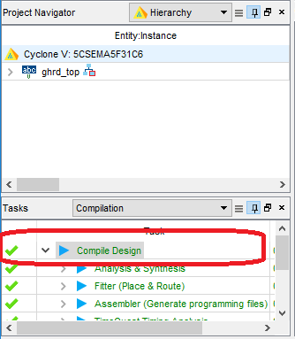
Double click on the “Compile Design” entry in the Tasks pane on the left. It will take roughly 15 minutes to build your system. If you encounter any errors, please fix these errors before proceeding.
Generating the Raw Binary File (RBF)
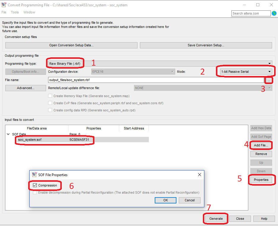
You now need to convert the default programming file type (.sof) to a raw binary format (.rbf). This is done using File?Convert Programming Files.
- Select a programming file type as Raw Binary File
- Select mode 1-bit Passive.
- Select a file name of output_files/soc_system.rbf
- Select Add File and navigate to output_files/soc_system.sof
- Click on Properties
- Select Compression
- Generate the File
Modifying Custom Peripherals
If you want to modify the behavior of your custom peripheral, you can open the Verilog file by expanding the ghrd_top instance in the Project Navigator, then expanding soc_system:u0, and then double clicking on example_peripheral:example_peripheral_0. After you have modified your Verilog code, you will need to re-compile the project and generate a new RBF file.
When Quartus generated the SoC system, it copied the files in .ipexample_peripheral into a directory called .soc_systemsynthesissubmodules . When Quartus compiles the project, it will synthesize the file in .soc_systemsynthesissubmodules.
IMPORTANT: If at any point you clean the Quartus project, you will want to copy the version of the file in .soc_systemsynthesissubmodules back to .ipexample_peripheral BEFORE you run the clean command. If you do not, any changes that you made after Qsys initially creates your system will be LOST!
Copy the FPGA programming image to A Micro SD Card
Now that you have an FPGA image built, we will use the Linux virtual machine to copy that image to the ?SD card. A boot loader (U-Boot) on the ?SD card will take care of programming the FPGA for us.
cp ./output_files/soc_system.rbf /media/ece453/SOC/soc_system.rbf
Testing Your Peripheral From U-Boot
1. You can test your peripheral by writing to the register set in the peripheral using the U-Boot command line. In the serial terminal, type the following commands to program the FPGA.
fatload mmc 0:1 $fpgadata soc_system.rbf;
fpga load 0 $fpgadata $filesize;
run bridge_enable_handoff;
2. Now that the FPGA is programmed, you can use the boot monitor to read and write memory locations in the HPS memory map. The boot monitor is a piece of code that is used to prepare a system to boot the operating system. The boot monitor can be used to initialize hardware devices, validating the system, and begins the Linux boot process.
The Altera Memory map tells us that the Avalon bus starts at physical address 0xFF20.0000. So let’s test your design by reading the Device ID register in your peripheral device.
md.l ff200080 10
You should see the following output
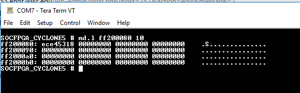
The device info is ece45318 which is the value found at the first register in your example_peripheral.v file.
3. If you change the values of the switches so that all the switches are in the up position, you will see the value of the second register change.
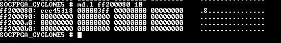
4. In order to change the value on HEX1, we will write a value of 3 to the gpio_out register.
mw.l ff200088 2
You should observe that a 2 is now displayed on HEX1.